Tutorial 9 | 6th Jan | 14:00 PM – 17:00PM (IST)
Digital and Analog/Mixed-Signal ASIC Design Flow with SCL 180nm PDK
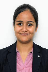
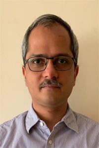
Speakers: Venkata Reddy Kolagatla, Shramona Roy and Vivian Desalphine, CDAC, Bangalore
About Speakers:


Venkata Reddy Kolagatla is a Principal Technical Officer (Scientist-D) working at C-DAC Bangalore for the past six years. Earlier, he worked with Synopsys India Pvt. Ltd. for one year as Senior Analog Design Engineer and prior to that, for three years at Sandisk India Pvt Ltd as Design Engineer II. He is Gold Medalist from the prestigious NIT Tiruchirappalli in his masters in the VLSI Systems specialization. He completed his B.Tech from JNTU Kakinada in Electronics and Communication Engineering. During his professional career at Synopsys and Sandisk, he worked on SDR/DDR1/DDR2/DDR3 industry standard Signal/Power Integrity aware IO Designs (Input receivers and Output transmitters) with Electrostatic discharge (ESD) and Latch-up considerations. His contributions involve design & development of peripherals (include Analog mixers, Duty Cycle Correctors, Frequency Dividers, Signal Drivers, On-Die Termination (ODT) Circuits, Calibration Circuits for Process Voltage & Temperature variations) for Single Data Rate (SDR), Double Data Rate (DDR), DDR2 and DDR3 speeds of 2D/3D NAND flash memories. Currently at C-DAC Bangalore, Mr. Venkat has worked in the areas of Cryptography, tamper resistant Crypto IP Cores Design, Development and Validation, System-On-Chip (SoC) Design and Development, SoC Peripherals such as Serial Peripheral Interface (SPI), Quad SPI (QSPI), Pulse Width Modulator (PWM), General Purpose Input Output Circuits (GPIOs), Timers, Watchdog Timer (WDT) Design and Implementation, Digital ASIC Physical Design and Physical Verification, etc. He played a key role in earlier SMDP C2SD project where he was instrumental in establishing RTL to GDS II IC Design flow using SCL 180nm PDK with the Cadence and Mentor EDA Tools. The experience gained was tremendously valuable in the physical verification of the various designs from academic institutes across the country. As part of Chip Centre, he led a team that carried out the physical design of SPI enabled AES Encryptor and IEEE 754 FPU (Single-Precision) Digital ASICs from RTL design to GDS-II generation using SCL 180nm foundry PDK and successfully completed the tapeout for both the designs to SCL Foundry. As part of ChipIN Centre activities under C2S Programme, he is involved in design and development activities targeting ASIC and technically supporting various academic institutes across the country. His technical strengths and interests include FPGA and ASIC based design and development, Analog and Mixed-Signal Design, IP core development of algorithms for Cryptanalysis/ Cryptography, Post Quantum Cryptography, Signal Integrity, and Power Integrity aware IO design, SoC design and development. He has numerous publications in reputed international journals and conferences, and he has presented at various seminars, workshops, and international conferences; he is widely recognized for his impactful research contributions.
Shramona Roy is a Project Engineer working at C-DAC Bangalore for the past two years. She completed her B. Tech and M. Tech in Electronics and Communication Engineering from IIITDM Kancheepuram specializing in VLSI Design. Shramona has been involved in research on Analog and Mixed-Signal circuit designs focusing on low-power applications in the fields of wearable electronics and edge IoT. Her research interests include artificial bio-neurons, neuromorphic encoders, PLL, ADC, and physical security and tamper resistance of sensitive chips. Her work has been published in various conferences and publications. Her paper on a low-power SAR ADC, using a novel RC DAC design, received the Honorable Mention Award at the 27th International Symposium on VLSI Design and Test (VDAT 2023). She is currently involved in the Chips-to-Startup Programme, heading the Analog/Mixed-Signal design team with the main objectives being to indigenously develop custom front-end ASICs and assist various academic institutions in training manpower in the field. She has worked extensively on the SCL 180nm technology node and has contributed significantly to establishing the SCL 180nm Analog/Mixed- Signal tool flow
Vivian Desalphine is an Associate Director at Centre for Development of Advanced Computing (C-DAC), Bangalore with around 19 years of experience. He is currently involved in Chips-to-Startup Programme, Design Linked Incentive and RISC-V based GPU development. He has been involved in various projects and programmes of national importance, viz. Microprocessor Development Programme, Chip-Centre for SMDP Chips-to-Systems Design, Cryptographic Module Validation Technologies, Enhanced Decryption Tool on Heterogeneous Platform, Design and Development of a Cooperative High Performance Traffic Generator for Time-Sensitive Network Analysis, Advanced Research in Ubiquitous Computing, Cryptanalysis: Novel Approaches and Intelligent techniques. His research interests include Computer Architecture, VLSI design and implementation, embedded processor subsystem design, caches, secure microprocessor architectures, SoC design, memory controllers, wired and wireless network media access controller design, hardware acceleration of domain-specific applications, ASIC & FPGA- based digital designs, etc. His professional experience includes Digital VLSI design and development, IP core design and development of hardware modules for RISC-V based microprocessor and GPU, FIPS 140-2 security compliant IP core design and development, IP integration and tapeout activities for Digital Design tapeout as part of Chip-Centre, IP core design and development of algorithms for Cryptanalysis/Cryptography, IP Core design and development for next-generation Gigabit (10GbE/40GbE) Ethernet MACs and IEEE 802.15.4 MAC hardware primitives, etc. He holds a B.Tech in Electronics and Communications Engineering from the University of Kerala, and has completed his Masters in Digital Signal Processing from the Department of Electronic & Electrical Engineering, University of Strathclyde, United Kingdom. His research has been published in several international conferences, and he has presented at various seminars, workshops, and international conferences. In addition, he has filed a patent and also been involved in numerous efforts towards industry transfer of technology.
Tutorial Abstract:
ChipIN Centre under Chips to Startup (C2S) Programme was set up at C-DAC Bangalore by Ministry of Electronics and Information Technology (MeitY), Government of India, to catalyze chip designing in India by catering to fabless chip design ecosystem in the country. The facility provides. Multi-Project Wafer (MPW) support to Academic Institutions, Startups and MSMEs by enabling access to SCL foundry and overseas foundries. It provides centralized EDA Design Tools (Synopsys, Cadence, and Siemens-EDA) for IC design flow. The facility also provides design services like Fab compliance checks, validation, integration of designs, coordinating with identified firm for packaging of fabricated chips and enabling characterization and prototyping in a centralized manner. A significant component of this effort is exposing Academia, Govt. R&D organizations, and Startups/MSMEs to the entire VLSI Design flow necessary to have their designs ready for fabrication at SCL/Overseas Foundries. This tutorial will walk through the entire design process for Digital and Mixed-Signal ASICs, from Logic/Schematic Design to final GDS-II generation, making use of EDA tools suggested by SCL Foundry. In the tutorial session, two case studies will be presented: Advanced Encryption Standard (AES) Digital ASIC and True Random Number Generator (TRNG) Mixed-Signal ASIC, both targeting SCL 180 nm CMOS process. The tutorial will cover the basics behind the working of the circuits while also building a solid understanding of the basics of the custom ASIC design process, including principles behind custom layout design for analog components and difficulties encountered during the process. Our team will additionally go into particulars about the various EDA tool features that a designer can use to best optimize the design flow. Cryptographic engines have started playing an indispensable part by ensuring data integrity, confidentiality, and security. These engines facilitate end-to-end encryption and authentication by safeguarding sensitive data from interception and tampering. It enables secure device-to-device communication, protect against unauthorized access, and build a strong foundation to build resilient and trustworthy applications. Any such engine requires a random key to perform different cryptographic operations. True Random Number Generators (TRNGs) are widely used as the source of random values for key generation. TRNGs exploit naturally occurring noise in electronic circuits such as clock jitters, quantization noise or thermal noise as the entropy source to generate confidential keys, initialize vectors, and random masks for all other encryption algorithms. This necessitates the need to design reliable, tamper-resistant and unbiased TRNGs as the most crucial part of any cryptographic engine. The tutorial will also cover standard statistical tests required to characterize the TRNG design discussed in the case study. Advanced Encryption Standard (AES) algorithm holds paramount importance in cryptographic engines due to its exceptional combination of security, efficiency, and widespread adoption. AES is a symmetric-key encryption algorithm that is considered highly secure against brute-force attacks when implemented with appropriate key lengths. Its efficient implementation on various platforms further solidifies its significance in cryptographic engines, enabling secure data protection without compromising system performance.


