Tutorial Day 1 | 26 Feb 2022 | Saturday
Track 1
Tutorial 1: Brain Inspired Computing: The Extraordinary Voyages from Known to Unknown Worlds
Speaker: Prof. Hai Li (Duke University)
Tutorial Abstract:
Human brain is the most sophisticated organ that nature ever builds. Building a machine that can function like a human brain, indubitably, is the ultimate dream of a computer architect. Although we have not yet fully understood the working mechanism of human brains, the part that we have learned in past seventy years already guided us to many remarkable successes in computing applications, e.g., artificial neural network and machine learning. Inspired by the working mechanism of human brain, neuromorphic system naturally possesses a massively parallel architecture with closely coupled memory, offering a great opportunity to break the “memory wall” in von Neumann architecture. The tutorial will start with a background introduction of neuromorphic computing, followed by examples of hardware acceleration schemes of learning and neural network algorithms and memristor-based computing engine. I will also share our prospects on the future technology challenges and advances of neuromorphic computing.
About Speaker:

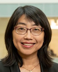
Hai Li
Dr. Hai “Helen” Li received her bachelor’s and master’s degrees from Tsinghua University, China, and her Ph.D. degree from Purdue University, USA. She is the Clare Boothe Luce Professor and Associate Chair of the Electrical and Computer Engineering Department at Duke University. Before that, she was with Qualcomm Inc., San Diego, CA, USA, Intel Corporation, Santa Clara, CA, Seagate Technology, Bloomington, MN, USA, the Polytechnic Institute of New York University, Brooklyn, NY, USA, and the University of Pittsburgh, Pittsburgh, PA, USA. Her research interests include neuromorphic computing systems, machine learning and deep neural networks, memory design and architecture, and cross-layer optimization for low power and high performance. She has authored or co-authored more than 250 technical papers in peer-reviewed journals and conferences and a book entitled Nonvolatile Memory Design: Magnetic, Resistive, and Phase Changing (CRC Press, 2011). She received 9 best paper awards and an additional 9 best paper nominations from international conferences. Dr. Li serves/served as an Associate Editor of a number of IEEE/ACM journals. She was the General Chair or Technical Program Chair of multiple IEEE/ACM conferences. Dr. Li is a Distinguished Lecturer of the IEEE CAS society (2018-2019) and a distinguished speaker of ACM (2017-2020). Dr. Li is a recipient of the NSF Career Award, DARPA Young Faculty Award (YFA), TUM-IAS Hans Fischer Fellowship from Germany, and ELATE Fellowship (2020). Dr. Li is an IEEE fellow and a distinguished member of the ACM.
Track 2
Tutorial 1: Event Cameras: From Biology to Circuits to Applications
Speaker: Prof Tobi Delbruck (INI/ETH Zurich/UZH)
Tutorial Abstract:
Conventional frame cameras have limited sample rate, limited dynamic range, and produce redundant output. Neuromorphic event cameras deal with these limitations by mimicking the asynchronous spike output of the eye to the brain. This tutorial video covers many aspects of event cameras: History, biology, pixel design, event readout, noise, processing algorithms, and some simple applications in high speed visual robotics. Participants to the Q&A session should come armed with specific questions about the tutorial.
About Speaker:

Tobi Delbruck
Tobi Delbruck (IEEE M’99–SM’06–F’13) received a B.Sc. degree in physics from University of California in 1986 and a Ph.D. degree from Caltech in 1993 in the inaugural class of the Computation and Neural Systems program founded by John Hopfield, as a student of Christof Koch, David van Essen and Carver Mead. Currently he is a Professor of Physics and Electrical Engineering at ETH Zurich in the Institute of Neuroinformatics, University of Zurich and ETH Zurich, Switzerland, where he has been since 1998. He directs the Sensors group together with Prof. Shih-Chii Liu. It focuses on neuromorphic event sensors and processing, with recent focus on theory and hardware accelerators for AI. He co-organizes the Telluride Neuromorphic Cognition Engineering workshop and has organized live demonstration sessions at ISCAS, NeuIPS, and AICAS and two Confession Sessions at ISCAS. Delbruck is past Chair of the IEEE CAS Sensory Systems Technical Committee. He worked on electronic imaging at Arithmos, Synaptics, National Semiconductor, and Foveon and has co-founded 3 companies inilabs, insightness, and inivation. He invented the neuromorphic adaptive photoreceptor circuit. The MOS pseudo resistor used in it is a key part of the most cited JSSC paper of the last decade in the neural-amplifier paper from R. Harrison. He also invented the “bump” circuit and open-source ultra wide dynamic range digitally programmable bias current generators used in many neuromorphic chips. His IEEE J. Solid State Circuits paper on the first dynamic vision sensor silicon retina event camera is the 4th most cited in the 2005-2015 decade. These event camera developments inspired the Sensors Group’s recent work on activity-driven AI hardware accelerators, e.g. NullHop and DeltaRNN, which are among the first to exploit neuromorphic activation sparsity for saving time and energy like spiking neural networks, but in a way that is much more compatible with DRAM storage of deep networks. His papers have been awarded 13 IEEE awards and in 2013 was named a Fellow of the IEEE Circuits and Systems Society for his work on neuromorphic sensors and processing. He likes to read storybooks, play tennis, and sometimes tries card magic on unwary subjects.
Track 1
Tutorial 2: SoC Architectures for accelerating AI Computing
Speaker: Bharat Daga (Intel)
Tutorial Abstract:
The proliferation of AI in various fields has resulted in exponential increase in the compute. This necessitates to rethink the compute architecture to keep pace with the demand for compute, memory bandwidth and inter process communication. In this tutorial, we will explore the various compute architectural solutions targeting AI workloads. The tutorial will delve into custom accelerators and various tradeoffs for performance and power.
About Speaker:

Bharat Daga
Bharat Daga is a Senior Principal Engineer and Director of Engineering, Habana Labs, Intel. He has an industry experience of over 24 Years in the field of Computer Architecture, AI/ML Hardware, CPU and VLSI design. For the last 8 years he has incubated and lead a design of AI/ML compute core targeting data centers and servers. He is the recipient of IAA – Intel Achievement Award the highest award in Intel for his pathbreaking work on AI/ML products. Bharat has a Masters in Computer Engineering from University of Delaware, USA and a bachelors from Osmania University, Hyderabad. He is a great sports enthusiast and regularly plays volleyball to keep fit.
Track 2
Tutorial 2: Event-driven low-compute bioinspired processing for Edge Audio
Speaker: Prof. Shih-Chii Liu (INI/ETH Zurich/UZH)
Tutorial Abstract:
This tutorial covers the design trend of ‘event-driven’ bioinspired or neuromorphic audio front-end circuits such as spiking silicon cochleas for edge audio devices that need to satisfy stringent power constraints of ‘always-on’ operation. These bioinspired circuits bypass the conventional combined stage of ADC and digital filtering. The microphone input signal is first processed by continuous-time analog bandpass filters followed by a rectification stage and a spike generation stage which produces binary asynchronous spikes. The spikes retain the asynchronous audio timing useful for tasks such as source localization. The features created from the spikes can be used to train deep neural networks for audio wake-up tasks including voice activity detection and keyword spotting. We show FPGA and ASIC examples of these audio devices for continuous small vocabulary speech recognition and keyword spotting.
Track 1
Tutorial 3: AI for Quantum, quantum for AI
Speaker: Nagendra Nagaraja (Qpi Technology)
Tutorial Abstract:
Quantum computers are based on Quantum mechanics representation of information using qubits. Quantum phenomenon like superposition, entanglement and Quantum interference. Quantum compute by its basic computation structure is massively parallel and can solve NP hard and combinatorial optimization problems better than classical compute. Hence problems in the area of drug discovery , transportation, Finance and manufacturing that are combinatorial optimization problems can be better solved using Quantum computers. But Quantum computers are in the hyperplane which need to be controlled by tuning various parameters of Qubits from the quantum control circuit. This is not possible manually or through adding more people at work. This is a problem that has to be solved by AI. So a Quantum computer to operate efficiently requires AI . Future of AI is in modelling intelligence efficiently using combination bits, qubits and neurons, this requires a Quantum computer to make AI more effective, Greener and sustainable .
About Speaker:

Nagendra Nagaraja
Dr Nagendra Nagaraja is a serial entrepreneur, who has raised $5 million USD in the past and currently is CEO , Chairman and Founder of QpiAI and its parent Qpi Technology. He has PhD in wireless and AI from Coventry university UK . He has a masters in Network engineering from Illinois Institute of Technology , Chicago and Bachelors of engineering from Bangalore university. He holds 25+ granted patents in wireless, AI, Quantum computing, security and multimedia and many more pending applications. He has a total of 22 years experience in the technology industry.
Track 2
Tutorial 3: On-Chip Memories – Challenges, Opportunities, and Recent Advances
Speaker: Prof. Manan Suri (IIT-Delhi), Anuj Grover(IIIT-Delhi)
Tutorial Abstract:
Estimates suggest that 463 exabytes of data will be generated daily in 2025. 175 Zettabytes of data storage is expected to be used in 2025. Already, 70-80% of area in advanced digital SoCs is occupied by memory. In this tutorial, we look at challenges and opportunities related to embedded memory circuit design and non-volatile memory devices. In advanced technology nodes, SRAM cell is co-designed across Technology and Design groups. First half of the tutorial will cover challenges related to read/ write operations in a conventional 6T SRAM cell and also give an overview of assist schemes used in design to gain density and functionality. Session will provide a glimpse of advanced statistical methods used in designing SRAMs. We introduce the memory bandwidth bottleneck in data-intensive applications and present some recent work on In-Memory Compute (IMC) in SRAMs. In the second session of the tutorial we will introduce basics and working of emerging Non Volatile Memory technology such as PCM (Phase Change Memory). Further, example case-studies of computational applications of emerging NVM devices, such as neuromorphic computing and logic-in-memory, will be briefly discussed.
About Speakers:

Manan Suri

Anuj Grover
Dr. Manan Suri leads the NVM and Neuromorphic Hardware Research group at IIT-Delhi. His research interests include Semiconductor Non-Volatile Memory (NVM) Technology and its Advanced Applications (Neuromorphic, AI, Security, Computing, Sensing). Dr. Suri has been globally recognized as a leading DeepTech Innovator. He was selected by MIT Technology Review as one of the world’s Top 35 Innovators under the age of 35 (MIT-TR 35 Global List – 2018) and Top 10 Indian Innovators under 35 (MIT-TR 35 India List – 2018). Dr. Suri received the prestigious IEEE EDS Early Career Award (2018), NASI Young Scientist Award (2017), IEI Young Engineers Award (2016), INAE Young Engineer’s Award (2021) and Laureat du Prix (2014) from the French Nanosciences Foundation. Dr. Suri has filed several patents, authored 85+ publications and successfully led several sponsored research projects as principal investigator. He has published at high impact venues such as Nature Communications, Scientific Reports, IEDM, TNNLS etc. Dr. Suri is the founder of IIT-Delhi Deeptech startup CYRAN AI Solutions which has developed multiple innovative technology products and solutions. He also serves as an advisor to leading AI/NVM Hardware companies and government bodies. In past, he has worked at NXP Semiconductors, Belgium as Senior Scientist and CEA-LETI, France. Dr. Suri received his PhD from INP-Grenoble, France and Masters/Bachelors from Cornell University, USA.
Dr. Anuj Grover is Associate Dean – IRD and Associate Professor in the Department of Electronics and Communication Engineering at Indraprastha Institute of Information Technology Delhi (IIIT Delhi). He also chairs the Institute Innovation Council and is a Level-3 Certified TRIZ Practitioner and frugal innovation enthusiast. Prior to joining IIIT Delhi in February 2019, Anuj worked at STMicroelectronics, India for about 18 years in different roles in the Embedded Memory Design team. Over the years he has led large teams on multi-million dollar projects. He has over 40 publications in peer-reviewed journals and conferences, 6 granted patents, and more than 10 invention disclosures in different stages of filing and grant. His main areas of research include low-power digital circuits and systems, embedded memory design, and reliable circuit design.
Track 1
Tutorial 4: Introduction to Memory technology & Products
Speakers: Kalyan Kavalipurapu and Venkat Bringivijayaraghavan, (Micron Technology)
Tutorial Abstract:
DRAM and NAND memory products play a key role in transforming the data processed by the various and diverse compute, communication and AI/ML systems into intelligence. This tutorial will provide an introduction to the DRAM and NAND semiconductor memory technologies and product designs highlighting some of their characteristics and challenges.
Part 1: “All about NAND Flash Memory”
Abstract:
The tutorial gives an insight into the basics of NAND flash, operations of NAND flash, 2D planar NAND and its evolution to 3D Floating gate and Replacement gate technology. Also discussed are the innovative CMOS under array technology, NAND performances and error correction features.
About Speaker:

Kalyan Kavalipurapu
Kalyan Kavalipurapu is Director, NAND Design, in Micron Technology, India.
Mr. Kavalipurapu joined Micron in July 2006, in the Non-Volatile Memory group in San Jose, CA, as an analog Design Engineer in NAND Design Team. Prior to that, Mr. Kavalipurapu Worked as Test Engineering Intern in Intel, Chandler, Arizona.
Mr. Kavalipurapu Spent the first thirteen years of his career in Silicon Valley, in various roles in NAND Design group, ranging from an individual contributor to integration lead. Mr. Kavalipurapu has authored and co-authored 20 patents till date. He moved back to India in 2019 and has taken up a challenging role as a Director- NAND Design, Building the team to deliver on NAND projects.
Kalyan earned his undergrad degree in Electronics and communication Engineering from Osmania University (India), followed by M.S. in Electrical Engineering from Arizona State University in Phoenix, Arizona.
Part 2: “An overview of the LPDDR4 architecture”
Tutorial Abstract:
This session will give an overview of the LPDDR4 architecture. Also, there will be a comparison between a compute, mobile and graphics DRAM family as the session navigates through the functional block diagram. This session will spur interests by sprinkling and highlighting some of the opportunities in the DRAM universe for the aspiring engineers.
About Speaker:

Venkatra Bringivijayaraghavan
Venkatraghavan Bringivijayaraghavan (“Venkat Bringi”) is a Director, Micron India and leads the DRAM and Emerging memory team. His 20+ years of industry experience spans around DRAM, SRAM & Register file development. In the past he has been associated with Micron Technology USA, IBM India, GLOBALFOUNDRIES India and Marvell India.
Venkat holds over 54 granted US patents (and several are pending) with many of his patents actively powering up several customer chips. He has mentored over a dozen team members with their debut patent and nurtured employees on technical leadership.
Venkat holds a master’s degree in Electrical and Computer Engineering, University of Nevada, LV, USA & Bachelor’s degree in Electronics & Communication Engineering, University of Madras. He is an undergraduate gold medalist.
Venkat is a recipient of IBM Innovation Excellence award & recognized as a Master Inventor at GLOBALFOUNDRIES. He was part of the Patent evaluation board, for the memory committee, at IBM, GLOBALFOUNDRIES and Marvell.
Track 2
Tutorial 4: HBM System and Architecture for AI applications
Speakers: Manish Jain and Nikhil Raghavendra Rao (Rambus)
Tutorial Abstract:
Artificial intelligence/machine learning (AI/ML) is impacting every industry and touching the lives of everyone. AI/ML’s evolution is proceeding at a lightning pace. Training capabilities are growing at a rate of 10X per year driving rapid improvements in every aspect of computing hardware and software. Memory bandwidth is one such critical area of focus enabling the continued growth of AI/ML. HBM memory is the ideal solution for the high bandwidth requirements of AI/ML training. The benefits of HBM make it the superior choice. The performance is outstanding, and higher implementation and manufacturing costs can be traded off against savings of board space and power. In data center environments, its lower power translates to reduced heat loads for an environment where cooling is often one of the top operating costs. This tutorial starts with the discussion on AI/ML driving high memory bandwidth requirements and creating need for innovative memory solutions (2.5D). It then describes HBM system components and its role. HBM performance evolution and how data rates have increased with each generation is discussed. It talks about HBM memory features, HBM PHY design and architecture key points, with emphasis on HBM3 designs. It covers system design, signal integrity and power integrity considerations for a HBM memory subsystem.
About Speakers:

Manish Jain

Nikhil Raghavendra Rao
Manish Jain is Senior Director of Engineering at Rambus, Bangalore. He is responsible for Serdes and Memory PHY development. He has spent 26 years in Semiconductor Industry, with over 17 years spanning at Rambus. He has designed Non-Volatile Memories, Analog Circuits and High-speed Analog Mixed Signal Circuits. His research interests include high-speed mixed-signal CMOS circuit design, transmitter and receiver design, equalization, PLL/DLL design and signal integrity analysis. He has received his B.E Degree in Electronics and Communication Engineering from Maulana Azad National Institute of Technology, Bhopal in 1995
Nikhil Raghavendra Rao is a Principal Engineer, Architecture at Rambus Bangalore. He is responsible for Memory PHY Architecture. He has 17 years of experience in the semiconductor industry and has worked primarily on Digital Design and Verification, SoC Design, FPGA prototyping, Graphics Memory (GDDR) PHY and HBM PHY Architecture. His research interests include Memory subsystem architecture, CPU architectures and Computer networking. He holds a Bachelors degree in Electrical Engineering from NIT Surat and a Master’s degree from Manipal University.
© 2021-2022, VLSID. All Rights Reserved.
Made proudly in India with ❤ by www.ConfiSpace.com


